
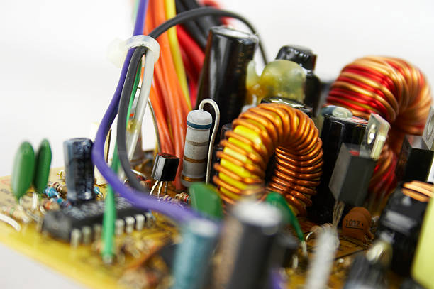
The PCB is the most fundamental component of any electronic design, and in recent times, it has developed to be extremely sophisticated components. There are various kinds of PCBs available in the market and each is manufactured according to its specifications along with their usages, specifications, and different types of materials utilized.
In the process of transforming how PCB industry shifts its focus to PC to high-frequency communication, smartphones, and other automotive electronic fields, the PCB manufacture and assembly industry is undergoing many shifts. As the PCBs are getting smaller, as more features are needed to be used, we have advanced PCB which offers accuracy and accuracy.
However, a large number of wholesalers and distributors require advanced PCBs these day, they are armed with limited or no knowledge of their production areas, application areas and order channels. In this article, we will talk the characteristics of advanced PCB and its uses, as well as its advantages and disadvantages.
What is a Advanced PCB?
Advanced electronic circuit boards (PCBs) are PCBs that have complex structures and more layers when compared to a standard multi-layer PCB.
Advanced PCBs have a greater electrical density per unit than traditional PCBs. They have better lines and spaces, as well as smaller through-holes, capture pads, and more connections pad density too.
Advanced PCBs can be found in a wide range of uses, particularly in electronic components that are high-end where precision and speed are extremely crucial, such as industrial equipment automotive Electronics Communications equipment, Medical facilities and the Military field.
Advanced PCB – 14 Layers
Applications of Advanced PCBs
Advanced PCBs are used in many industries compared to the standard PCBs. Modern printed circuit boards have many applications in various areas, including:
- Industrial equipment Advanced PCBs are employed in these fields to ensure greater precision as well as the safety of employees and a faster functioning of the equipment.
- Automotive Electronics – The use of modern PCBs lets you store the full array of exquisite sensors and other components required for the continuous performance of a car.
- Communication equipment – To route signal and electricity, sophisticated PCBs are required to operate in this area.
- Medical equipment – Advanced PCBs are utilized in conjunction with medical equipment in monitoring body temperature or heart-related devices.
- Military field – They are essential to the functioning of military navigation, guidance and the control of war equipment.
Type of Advanced PCB
In the case of advanced PCBs the number of layers is crucial because it directly impacts the performance. For instance double-layer high-level PCBs be more efficient than one-layer PCBs that are advanced.
The following are the different types of advanced PCBs:
- Multilayer Boards It is composed of three or more double-sided panels stacked over each other. In theory, they could contain more plates than are required.
- Flexible and rigid boards PCBs that are rigid consist of rigid boards that are unable to bend and are commonly used in situations where bent is not needed. Flexible boards are able to bend easily and are utilized in cases where bending is required to make electronic gadgets.
6-Layer Rigid-Flex
- Boards with high-frequency These PCBs are able to transmit high-frequency signals, mostly over 1GHz. They can be quite expensive.
Advanced PCB Design and Manufacturing
The process for designing Advanced PCB is similar to the one of the conventional PCB design. The IPC-2221A standard for general purpose is also followed.
You can utilize any PCB design program to design the PCB layout, but it’s a little more complicated than conventional PCB.
The process of manufacturing advanced PCBs is similar to the process used in the multilayer type of PCB. But the materials employed in both is different. Because the Advanced PCBs operate in areas in which heat and power are extremely high, these PCBs need materials that are able to be able to handle heat and power efficiently.
In modern PCBs, the identical Reflow Soldering and Wave Soldering PCB Assembly Processes are carried out with high precision because of its small dimensions and the high number of electronic parts.
Challenges
There are a few challenges associated encountered by Advanced PCB are listed below:
- The latest PCB technology is more expensive than conventional PCBs.
- Few manufacturers have the necessary technology to make PCBs with unbeatable density.
- The circuits with higher density tend to be more susceptible to conductive path defects in the manufacturing process, which causes rejection of the products that are finished.
- Methods for fixing the damaged conductor paths are costly, complicated and limited. They are also slow.
- Continuous pursuit of smaller electronic devices is further enhancing the limitation.
Comparison Between Advanced PCB and Standard PCB
Advanced PCB Manufacturer
When you are purchasing your high-end PCBs it is important to pick the right manufacturer. You don’t wish to partner with a company who has no expertise in the production of Advanced PCBs. In the end, you’re paying for your hard-earned cash, and therefore, you should be expecting superior boards.
If you’re looking an experienced company to create advanced PCBs for you look no further than PCBWay.com. PCBWay is among the most seasoned PCB manufacturing companies based in China with experience more than 10 years in the area of PCB prototyping and manufacturing.
PCBWay has created a distinct advanced PCB manufacturing workshop to help their customers receive their PCBs at the lowest cost, along with speedy delivery and top quality products.
You can purchase your Advanced PCB through PCBWay via click here.
PCBWay has come up with a brand new and exciting feature for all of its customers, collaborating with KiCad.
Once you’ve completed your design using KiCad then you are able to make your purchase via PCBWay by using only one